Why Do Solar Panels Lose Power After Installation? Understanding the LID Effect
You have installed the latest technology solar panels on your rooftop. Everything is working fine and you are enjoying the smooth electricity, but suddenly, after one month, you noticed that your solar panels are making 4.9 kW instead of 5 kW.
Is something wrong with your solar panels?
Or is there any problem with the system design?
Don’t worry, it could be due to the LID effect.
In this blog post, we’ll understand how LID affects the performance of the solar panels.
LID Effect Explained
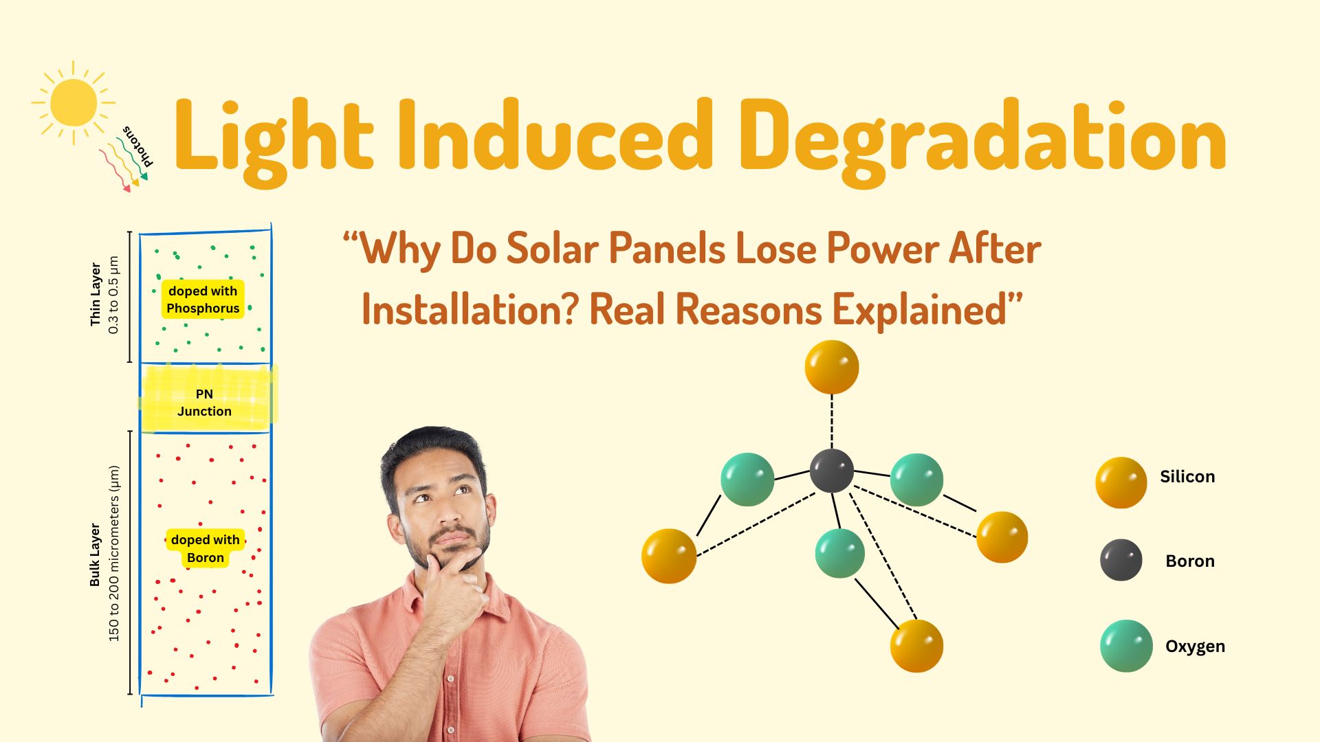
LID is the light-induced degradation that affects the solar panel’s performance within the first few hours of its exposure to sunlight.
The solar panel power can drop up to 2-3% of its Pmax, and this loss is permanent.
☀️Interested in knowing more about Solar Energy? Join My Master Class Today!
How does it happen?
The boron present in the silicon cell reacts mainly with trapped oxygen to form a Boron-Oxygen compound. This complex compound then inhibits the PV effect by increasing the recombination rate.
How does oxygen get trapped in the cell?
For this, we need to understand the Czochralski process.
The Czochralski process is named after Jan Czochralski, a Polish scientist.
🇵🇱 Country: Poland
🧪 Profession: Chemist and metallurgist
📅 Born: 1885, Kcynia, Poland (then under Prussian rule)
🧬 Contribution: In 1916, he accidentally discovered the method for growing single crystals while studying metal crystallization—now known as the Czochralski method, widely used in semiconductor and solar industries.
The Czochralski Process
The Czochralski process is a crystal-growing method in which a seed crystal is slowly pulled and rotated from molten silicon to form a large, pure single-crystal silicon ingot used in solar cells.
Explaination
A silicon crystal is grown by dipping a seed crystal into molten silicon and slowly pulling it out while rotating.

When we pull the seed upwards very slowly while rotating it, the molten silicon in the crucible (made of quartz) begins to stick to the seed uniformly. The crystal starts growing radially and axially from the seed as it is slowly pulled up, maintaining the same lattice orientation.

Because the seed is slightly cooler than the molten silicon, atoms from the melt solidify on it in the same crystal structure. With this process, we can get a pure silicon cylindrical ingot of length as large as 2 m and diameter up to 30 cm.

But during this process of crystallization, some oxygen from the quartz crucible (made of SiO₂) gets trapped in the seed.
Thereafter, this large seed is cut into wafers of size 18.2 cm x 18.2 cm standard solar cells.

Oxygen as a Impurity
The molten silicon used in the Czochralski process is contained in a quartz crucible (made of SiO₂). This setup introduces some oxygen impurities into the growing silicon crystal, which may seem undesirable at first.
So, why do we still use quartz crucibles despite this?
While alternatives exist, quartz remains the preferred material due to a combination of critical advantages:
- It has a high melting point of ~1700°C, which is suitable for molten silicon.
- It is chemically compatible and does not contaminate the molten silicon with other metal impurities, unlike many other materials.
- A quartz crucible is transparent to Infrared, which helps in maintaining the right temperature for crystallization.
- It is cost-effective, relatively cheap, and readily available.
Although it introduces some oxygen into the crystal, controlled oxygen levels can improve mechanical strength and resist dislocation formation in some applications.
Therefore, quartz crucibles offer an optimal trade-off between performance, purity, and cost.
Does LID affect all types of solar panels equally?
No, it affects P-type Monocrystalline solar panels the most, which use Boron as a dopant.
What is P-type solar cell?
Pure Silicon by itself is not efficient enough to convert sunlight into electricity. Because it has very few free charge carriers (electrons or holes). And when sunlight falls, it produces a tiny current.
Additionally, pure silicon does not have a PN junction. Whatever, electrons and holes are generated when sunlight falls on it, and most of them recombine again without constituting any current.
Hence, a lot of sunlight is wasted in heat and recombination instead of generating electric current.
Therefore, to make it effective and efficient, we dope it with impurities, either Boron or Phosphorus.
- When silicon is doped with Boron (tri-valent impurity), we get a P-type solar cell.
- And doping it with Phosphorus (penta-valent impurity), we have an N-type solar cell.
Read: P-Type vs N-Type Solar Cells
Also, doping with either of the impurities results in the formation of a PN junction. This PN junction creates an electric field inside the cell, which prevents the electrons and holes from recombining (generated when sunlight falls on the cell) and creates a flow of electric current when the solar cell is connected across the load.
A P-type solar cell is formed when the bulk layer of silicon (150–200 µm) doped with Boron is combined with a thin silicon layer (~0.3–0.5 µm) doped with Phosphorus.

The resultant solar cell is P-type, creating an abundance of positive charge carriers (holes).
The Formation of Boron-Oxygen Compond
When the P-type monocrystalline solar cell is formed through crystallization (Czochralski Process), the oxygen gets trapped in the crystal.

And when this solar cell is exposed to the sunlight, the trapped oxygen reacts with the Boron to form complex Boron-Oxygen compounds, which facilitate the recombination of the holes and electrons. Hence, reduces the free electrons available to constitute current.
How to avoid LID effect in Solar Panels?
(1) Use gallium-doped mono-PERC solar panels instead of boron-doped ones, as gallium does not form recombination-active defects with oxygen. Gallium-doped solar panels cost slightly more, but for the consumer, they offer better value for money over the long term (due to reduced LID effect and improved long-term performance).
The manufacturers can lower the LID effect in the Boron-doped solar panels by optimizing the Czochralski Process by:
- Lowering the pulling rate
- Using a higher quality Quartz crucible
(2) Avoid long-term exposure to high temperatures after installation. As high temperature and light can reactivate some B-O defects in the modules. I know that one cannot avoid the temperature effect beyond a certain limit. But ensuring proper ventilation between the panels at the time of installation can help in reducing the reactivation of B-O defects.
How do I check whether my solar panels are Boron-doped or Gallium-doped?
(1) Look under the “cell technology” section in the datasheet. Look for the keywords like:
- Gallium-doped
- Boron-doped
- LID free or LID resistant (often implies gallium doping)
(2) Observe the degradation warranty
- Boron-doped solar modules often have higher degradation, like 2-3% in the first year and then 0.55% – 0.7% per year thereafter.
- While Gallium-doped models often have <2% degradation in the first year and thereafter 0.4 – 0.45%.
(3) Clue
- If the power output is 84-85% after 25 years, it is most likely Boron-doped.
- While Gallium-doped solar modules give power 87.4% after 25 years.
Mono-PERC technology typically uses boron-doped Cz-Si wafers, unless explicitly noted as gallium-doped.
Manufacturers usually highlight “gallium-doped” or “LID-free” if they’ve switched to gallium, especially as part of marketing or technical specs.
With no mention of gallium, it’s safe to assume it’s boron-doped.
How does LID affect other cell types?
LID (Light-Induced Degradation) does not affect all types of solar panels equally.
It mainly depends on the type of silicon used and the dopant (Boron or Gallium). Let us look at the table below to know the LID effect on different cell types:
| Solar Cell Type | Dopant | LID Impact | Why? |
| P-type Monocrystalline | Boron | Yes (1–3%) | Boron reacts with oxygen → boron-oxygen complex → initial power loss. |
| P-type Multicrystalline | Boron | Yes (Moderate) | Similar issue, though less uniform than mono. |
| P-type Monocrystalline | Gallium | No / Very Low | Gallium does not react with oxygen → No LID. |
| N-type Monocrystalline | Phosphorus | No / Negligible | Different structure; LID-resistant, stable over time. |
| Heterojunction (HJT) | N-type base | No | Uses N-type wafer + amorphous silicon layer – LID is absent. |
| TOPCon | N-type base | No / Very Low | Improved passivation – LID impact is minimal. |
| Thin-Film (CdTe, CIGS) | — | Not Affected | These are non-silicon technology → no boron/oxygen to cause LID. |
Summary
Light-Induced Degradation (LID) is a natural phenomenon that causes a 2–3% permanent drop in power output within the first few hours to days of sunlight exposure, especially in boron-doped P-type monocrystalline solar panels.
It is mainly caused by the formation of boron-oxygen complexes, due to oxygen impurities introduced during the Czochralski process.
To reduce or avoid LID:
- Opt for gallium-doped panels or N-type technologies like TOPCon or HJT, which are LID-resistant.
- Buy from reputed manufacturers offering solid warranties and efficiency ratings.
While LID is real, it’s manageable. For most homeowners, it’s not a major concern if the system is designed and installed properly with reliable components. Lastly, standard boron-doped P-type panels are still a great, cost-effective choice if bought from reliable brands with warranties that account for LID.


