PN Junction in a Solar Cell: Simple Explanation, Diagram & Working
Introduction
When I was in the first year of my Engineering (Electronics & Communication), the PN junction was one of the first concepts I learned.
At that time, I never imagined that years later, I would be teaching the same concept to thousands of homeowners, solar enthusiasts, and even M.Tech students through this blog.
Funny how life connects the dots, right?
Back then, the PN junction felt like just another semiconductor topic — something to pass the exam.
But today, I see it as the heart of every solar cell.
Without the PN junction, a solar panel simply cannot produce electricity.
So, in this article, let’s break it down in the simplest possible way:
What is a PN junction, what happens inside it, and how does it help a solar cell convert sunlight into usable electricity?
Let’s begin.
What Exactly Is a PN Junction? (With Doping Explained Clearly)
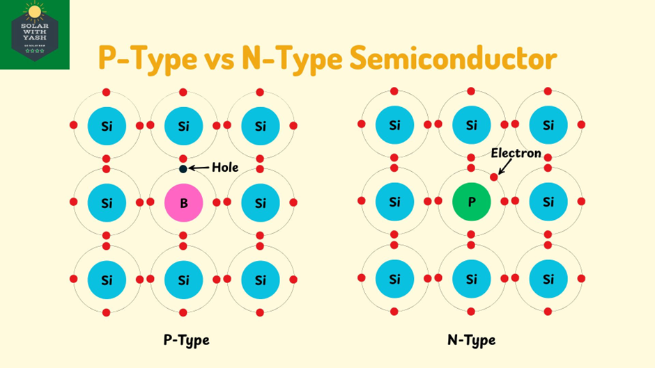
To understand the PN junction, we first need to understand how P-type and N-type semiconductors are created.
A. How a P-type Semiconductor Is Formed
- Start with pure silicon.
- Add a small amount of Boron (B) — a trivalent impurity (3 valence electrons).
- Silicon has 4 valence electrons, so when Boron mixes with silicon, it forms 3 bonds, but one bond is incomplete.
This incomplete bond becomes a hole.
✔ Key idea:
A P-type semiconductor has:
- Lots of holes (positive charge carriers)
- Very few free electrons
This region behaves as if it is “positive” because holes dominate the conduction.
B. How an N-type Semiconductor Is Formed
- Start again with pure silicon.
- Add a small amount of Phosphorus (P) — a pentavalent impurity (5 valence electrons).
- Phosphorus forms 4 bonds with silicon, and one extra electron is left free.
This extra electron becomes the free charge carrier.
✔ Key idea:
N-type semiconductor has:
- Lots of free electrons (negative charge carriers)
- Very few holes
This region behaves as “negative” because electrons dominate the conduction.
Below is the visual structure of P-type and N-type semiconductors.
I used the same diagram earlier in “What is a Semiconductor?”,
And I’m adding it here for clarity because everything starts with doping:
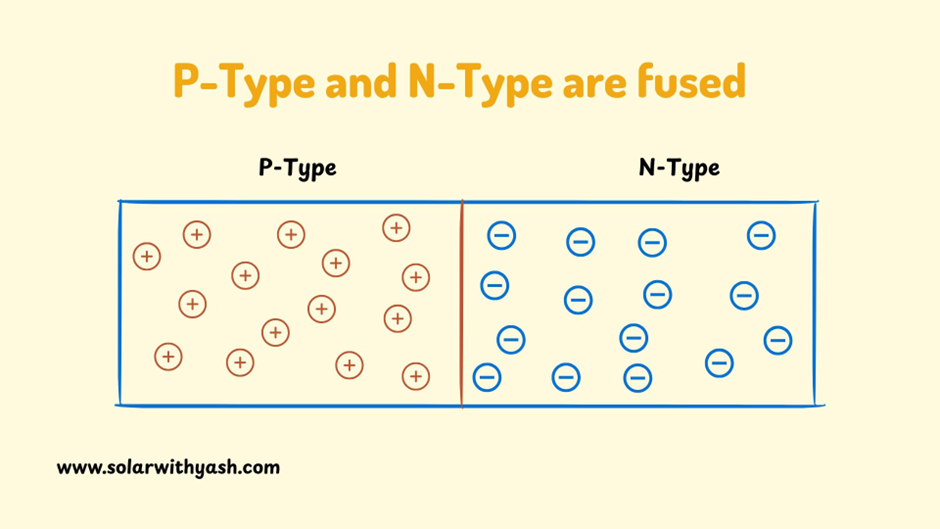
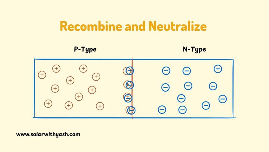
C. Now, let’s join the two worlds together
Think of it like joining two very different neighbourhoods:
- One side (P-type) has too many holes
- The other side (N-type) has too many electrons
When we bring them into contact, something happens instantly:
- Electrons from the N-side rush into the P-side
- Holes from the P-side move into the N-side
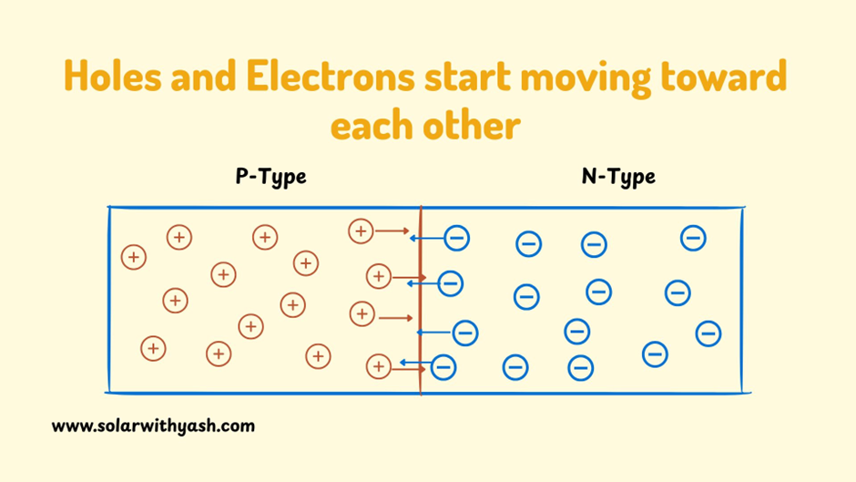
This movement continues until they recombine and neutralize each other near the boundary.

The formation of Depletion Region
D. The boundary becomes empty → the Depletion Region
Because recombination eliminates free carriers near the junction, this region becomes:
- Empty of free electrons
- Empty of free holes
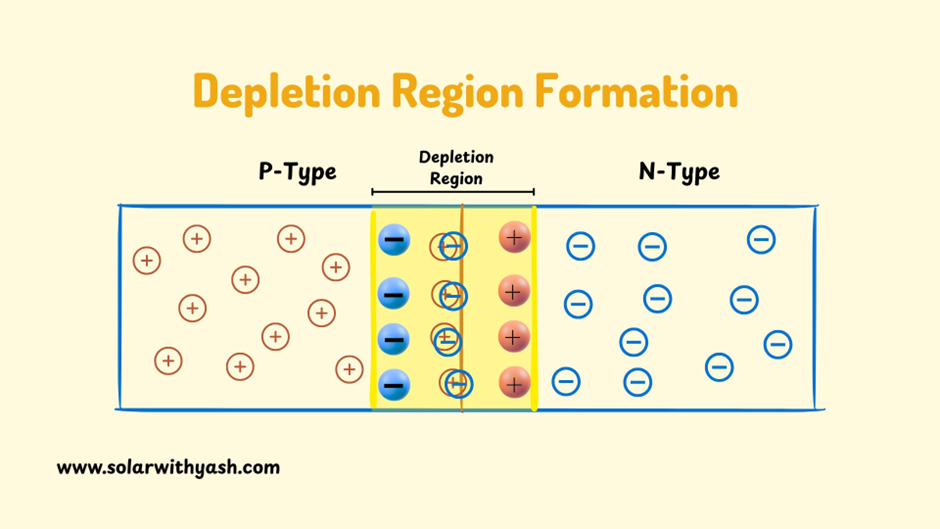
Hence the name “Depletion Region” — a region “depleted” of charge carriers.
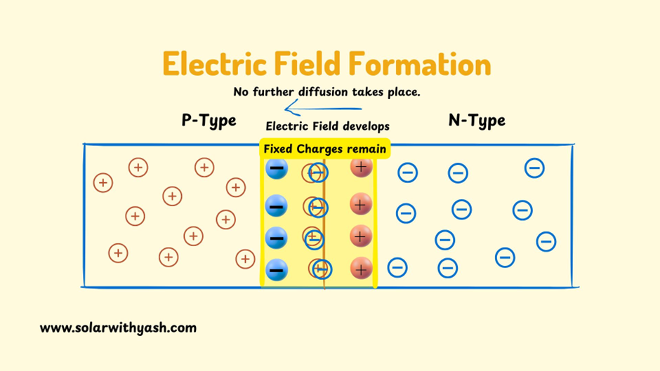
But the atoms left behind (ions) create fixed charges, forming an electric field. This electric field is the MOST important part of a solar cell.
E. One line summary of the PN Junction
A PN junction is simply the boundary formed when a P-type and an N-type semiconductor are joined together, creating a depletion region and a built-in electric field that separates charges.
This internal electric field is what makes solar cells generate electricity.
The Depletion Region — The Most Important Part of the PN Junction
Once the P-type and N-type materials are joined, electrons and holes start to recombine near the boundary.
This recombination empties the region around the junction.
This “emptied” zone is called the Depletion Region.
Let’s break it down step by step so you understand it exactly the way I did in my engineering days.
A. What actually gets “depleted”?
Two types of charge carriers:
- Free electrons (from the N-side)
- Free holes (from the P-side)
These two annihilate each other as soon as they meet.
The result?
A region with:
❌ No free electrons
❌ No free holes
✔ Only fixed, immobile ions
That’s why it is called the depletion region.
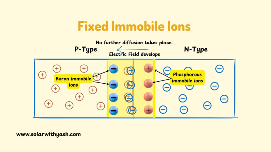
B. Why ions remain behind
When electrons leave the N-side:
- They leave behind positively charged donor ions (Phosphorus atoms without the extra electron)
When holes leave the P-side:
- They leave behind negatively charged acceptor ions (Boron atoms that captured an electron)
These ions cannot move.
So, the depletion region becomes a zone filled with fixed positive and negative charges arranged on either side of the junction.
C. This creates an internal electric field (the key to solar electricity)
Because of the fixed charges, an electric field develops:
- Direction → from N-side (positive ions) to P-side (negative ions)
This electric field acts like a built-in sorting machine:
- It pushes electrons toward the N-side
- It pushes holes toward the P-side
This separation of charges is the heart of the photovoltaic effect. Without this field, sunlight would still generate electron-hole pairs…
but they would IMMEDIATELY recombine → zero electricity.
D. Built-in Potential (Vbi)
The electric field creates a natural voltage across the junction:
For silicon (used in solar cells):
- 0.6 – 0.7 V approximately
This is called the built-in potential.
It’s not used to power devices directly, but it drives charge separation, which ultimately gives us voltage and current in the solar cell.
E. Width of depletion region
The width depends on:
- Doping concentration
- Temperature
- Semiconductor material
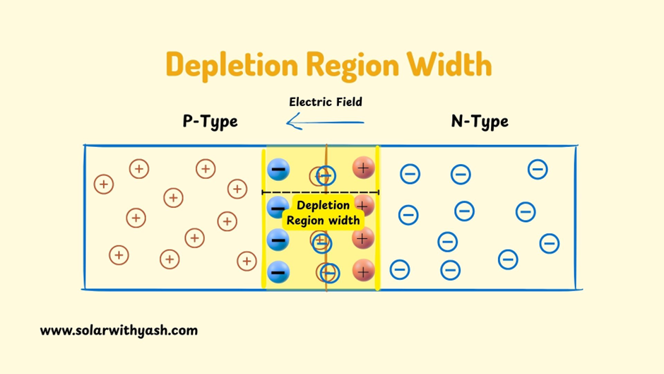
Highly doped → thinner depletion
Lightly doped → wider depletion
This is important because wider depletion regions collect more light-generated carriers, improving efficiency.
INNOVATIVE ANALOGY — “Hot Air Meets Cool Air at a Doorway”
Imagine two rooms separated by a door:
🔵 Room N (N-type) → Filled with hot air
→ (Hot air molecules = electrons with high energy & high concentration)
🔴 Room P (P-type) → Filled with cool air
→ (Cool air = region with fewer electrons = holes dominate)
Understanding the Analogy
⭐ Step 1: You open the door between the two rooms
What happens instantly?
Hot air rushes into the cool room.
This is exactly like:
- Electrons moving from N-type → P-type
At the same time…
Cool air flows into the hot room
This is like:
- Holes (low-energy regions) moving from P-type → N-type
⭐ Step 2: The mixing happens right at the doorway
Hot & cool air mix only near the boundary.
This mixing zone becomes:
- No hot air
- No cool air
Just neutral, uniform air.
This is the depletion region.
No electrons.
No holes.
Just an empty, neutral zone.
⭐ Step 3: Pressure builds near the doorway
After a few seconds:
- The hot room loses some hot air → pressure drops
- The cool room gains hot air → temperature rises slightly
This creates a pressure difference across the doorway.
This pressure difference represents:
- Fixed ions
- Electric field
- Built-in potential (around 0.6–0.7 V for silicon)
This pressure acts like an invisible barrier.
⭐ Step 4: The doorway becomes a “one-way air gate”
Because of the pressure difference:
- Hot air cannot freely flow into the cool room anymore
- Cool air cannot freely enter the hot room anymore
The boundary has now become a control point that pushes air back to its own side.
This is exactly what the electric field does in a PN junction:
- Pushes electrons to the N-side
- Pushes holes to the P-side
⭐ Step 5: The final stable zone — same as PN junction equilibrium
Eventually, the doorway stabilizes:
- Air movement stops completely (equilibrium)
- A strong pressure difference remains
- Hot and cool air stay mostly on their sides
This is exactly the state of a stable PN junction:
- Depletion region formed
- Built-in electric field established
- Charges separated naturally
⭐ Analogy Mapping (Super Clear)
| Real PN Junction | Analogy |
|---|---|
| Electrons | Hot air molecules |
| Holes | Cool air region / low-energy air |
| PN junction | Door between rooms |
| Recombination | Mixing of hot & cool air |
| Depletion region | Neutral temperature air near the doorway |
| Ions left behind | Pressure difference across the doorway |
| Electric field | Force created by pressure difference |
| Built-in voltage | Temperature/pressure imbalance |
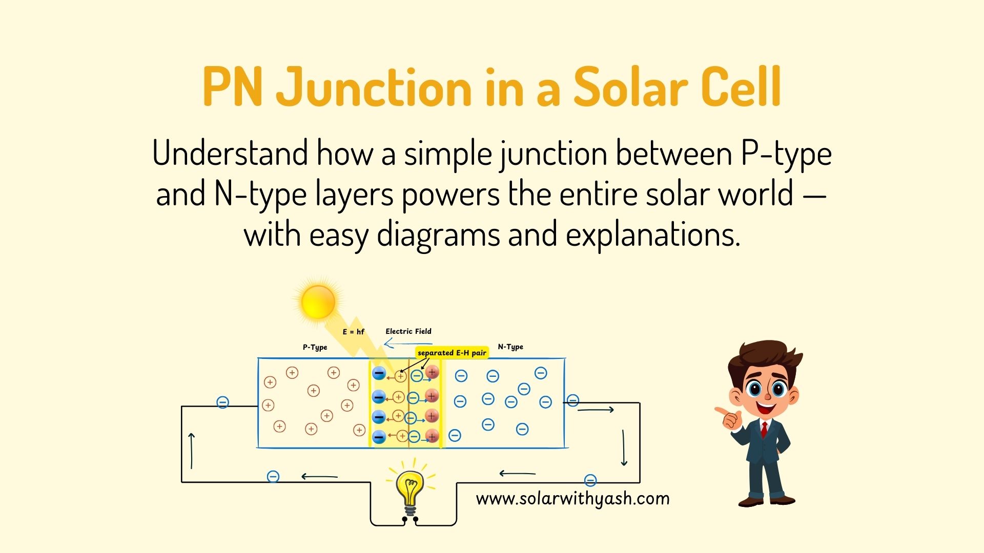
How the PN Junction Works Inside a Solar Cell (Sunlight → Charge Separation → Current)
Now that we understand how a PN junction forms and how the depletion region creates an internal electric field, let’s add sunlight into the picture and see how electricity is actually produced.
This is where the magic of solar power begins.
⭐ A. Step 1: Sunlight Hits the Solar Cell
Sunlight is made of tiny energy packets called photons.
When these photons strike the silicon atoms inside the solar cell, they transfer their energy to electrons.
If the photon energy is high enough, it breaks the electron out of its bond, creating:
- One free electron (negative charge)
- One hole (positive charge)

This pair is called an electron–hole pair (EHP).
This is the basic photovoltaic action.
⭐ B. Step 2: EHPs Get Created Near the Depletion Region
Most electron–hole pairs need to be created within or near the depletion layer.
Why? Because only there the internal electric field exists.
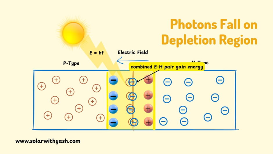
If the EHP is generated far away, the electron and hole will recombine before they can be collected. Good solar cells are designed so that most sunlight is absorbed near the PN junction.
⭐ C. Step 3: The Electric Field Separates the Charges
Remember the “hot and cool air pressure difference” analogy?
That internal electric field at the PN junction behaves like a sorting machine:
- It pushes electrons toward the N-side
- It pushes holes toward the P-side
This is the MOST important step.
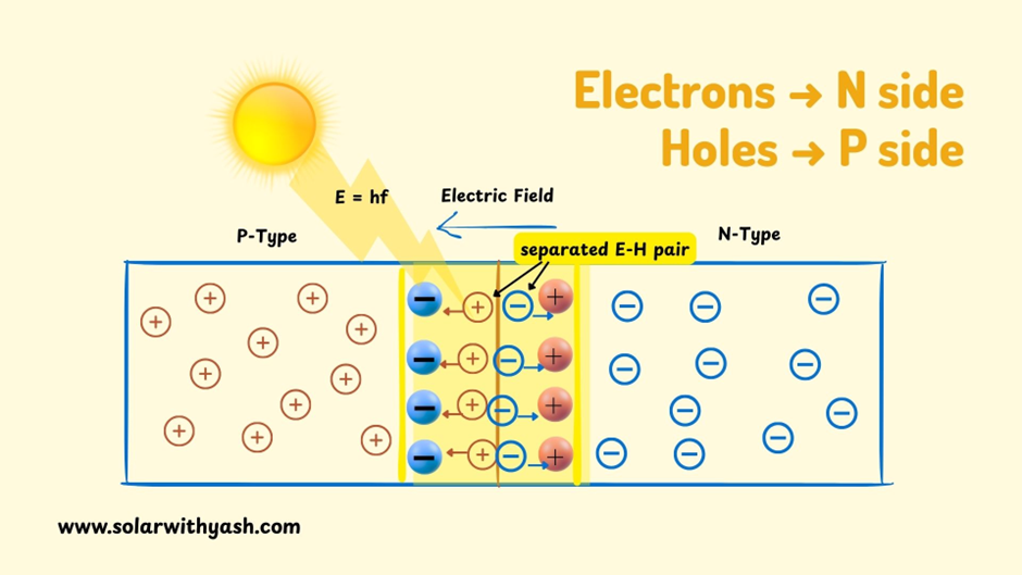
If the junction didn’t have this electric field, electrons and holes would simply recombine → zero electricity.
The PN junction “pulls them apart” before they recombine.
⭐ D. Step 4: Charges Move into the External Circuit
After separation:
Electrons move:
N-side → metal contacts → external wires
Holes move:
P-side → metal contacts → external wires (as positive current)
Electrons travel through the external circuit, powering:
- a home
- a battery
- an inverter
- or any load
and return back to the P-side of the solar cell.
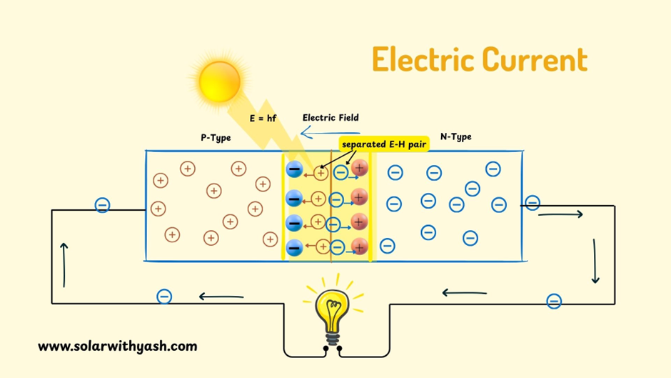
This movement of electrons through the circuit = electric current.
⭐ E. Step 5: Voltage Appears Across the Solar Cell
Because the electric field pushes charges in opposite directions, the solar cell develops a measurable voltage:
- Typically, 0.5–0.7 V for a single silicon solar cell
To get a useful voltage, multiple cells are connected in series:
- 36 cells → around 18V (for 12V systems)
- 60 cells → around 30V
- 72 cells → around 36V
This voltage is what your solar panel delivers to your inverter.
⭐ F. Step 6: Power = Voltage × Current
Once both voltage and current are present:
Your solar panel is producing useful electrical power from sunlight — thanks entirely to the PN junction.
⭐ G. Summary of the Whole Process (Very Simple)
- Sunlight hits the cell
- Electron–hole pairs are created
- The depletion region’s electric field separates them
- Electrons go to the N-side, holes to the P-side
- Electrons flow through wires → electricity
- Voltage is produced due to the built-in field
- Power is delivered to your home
Everything depends on that one tiny PN junction.
Want to learn how solar cells actually work — from PN junctions to full solar systems?
🎓 Join my Solar Energy Masterclass: Basics to Profit — Learn Basics, Design Smart, Size Right, and Profit Big!
Conclusion
A PN junction is the core of a solar cell.
When P-type (hole-rich) and N-type (electron-rich) semiconductors join, electrons and holes recombine near the boundary, forming a depletion region.
This region develops a built-in electric field that naturally separates charges generated by sunlight.
As electrons move to the N-side and holes to the P-side, a voltage appears and current flows through an external circuit.
This simple PN junction is what makes the entire solar photovoltaic effect possible.
Frequently Asked Questions on PN Junction in solar cell
1. What is a PN junction in a solar cell?
A PN junction is the boundary formed when a P-type and N-type semiconductor are joined. It creates a depletion region and an internal electric field that separates electrons and holes generated by sunlight.
2. Why is the PN junction important for a solar cell?
Because it provides the electric field needed to push electrons to the N-side and holes to the P-side. Without this separation, no current would flow and the solar cell wouldn’t work.
3. What is the depletion region?
It is the region near the junction where free electrons and holes have recombined, leaving behind fixed ions. This region has an electric field that drives charge separation.
4. What is built-in potential (Vbi)?
It is the natural voltage across the PN junction due to the electric field in the depletion region. In silicon solar cells it is typically 0.6–0.7 volts.
5. How does light generate electricity in a solar cell?
Sunlight generates electron–hole pairs. The PN junction’s electric field separates these charges, and electrons move through the external circuit to produce electricity.
6. What is band bending in a PN junction?
Band bending happens when the Fermi levels of P and N regions align at equilibrium. The bending creates a potential barrier and an electric field that separates charges.